Scientists at the University of California, Santa Barbara have shown that engineered spins in lab-grown diamond can be entangled and squeezed to beat classical limits for precision measurements. In simple terms, they made diamond-based sensors more accurate than what classical physics allows by using quantum tricks. This advance could lead to compact, extremely sensitive devices for measuring magnetic fields, time, and other physical quantities.
How spins in diamond work as sensors
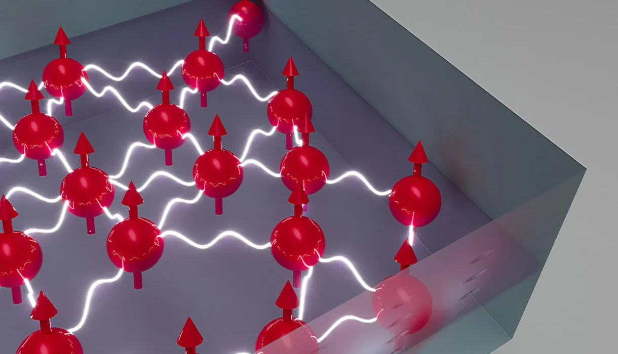
Diamonds can harbor tiny defects, called nitrogen-vacancy (NV) centers. Each NV center acts like a single quantum spin that responds to magnetic fields and temperature. Already today, single NV spins are used as tiny sensors that work at room temperature. The new work goes a crucial step further: instead of using separate and independent spins, the researchers created a two-dimensional layer of densely packed spins and made them interact. These interacting spins can be entangled and squeezed, which decreases the measurement noise and enhances sensitivity.
What is quantum squeezing, and why does it help?
Quantum squeezing is one of the ways to decrease uncertainty in a measurement by accepting more uncertainty in another, as allowed by Heisenberg’s uncertainty principle. In many sensors, that key noise is within one variable, such as the angle of a spin. By squeezing that variable across many spins collectively, the readout becomes cleaner. The UCSB team engineered dipolar interactions and controlled the spins’ geometry so that squeezing and entanglement naturally emerged, giving a measurable advantage over classical, unentangled sensors.
Why this matters: Real-world sensors, not just lab toys
One of the major barriers to quantum sensing, though, has been that most quantum tricks only work in delicate lab settings, and at low temperatures. NV centers in diamond are special because they can operate at room temperature and in ordinary conditions. By demonstrating entanglement and squeezing in a solid diamond platform, the UCSB team moved quantum advantage into a practical material; thus, future devices could be compact, robust, and deployable outside of the lab, for medical imaging, underground mapping, or precision navigation.
How they did it - engineering the diamond
They grew diamonds with a controlled layer of defects confined near the surface, tuning the density, orientation, and depth to realize a two-dimensional interacting layer. The spins were driven into correlated states by microwave and optical control, and the resulting noise suppression was measured. Careful material engineering and control pulses made the difference: the spins were interacting strongly enough to entangle but also accessible for optical readout. This balance is key to turning a quantum idea into a usable sensor.
Near-term applications to watch for
- Magnetic field imaging: More precise, handheld magnetometers for medical and geophysical applications.
- Navigation: Compact quantum sensors may enable navigation in GPS-denied environments by measuring minute changes in the Earth’s field.
- Material science and industry: detection of tiny defects or currents in electronics.
- Fundamental physics: Ultra-sensitive searches for weak signals, such as dark matter interactions or exotic forces.
Because the platform is solid state and operates near room temperature, industry adoption is more realistic and faster than many other quantum technologies.
Limits and next challenges
Despite the advance, several challenges remain: sustaining entanglement over many spins long enough for a measurement where noise, temperature variations, and material defects can reduce that time; and scaling up without compromising the fidelity of control. Integration of such diamond sensors with compact electronics and readout optics will need additional engineering effort. Nevertheless, the proof of principle is given: quantum advantage in a practical solid-state material is possible, and it is being engineered.
Watch to know more
Conclusion
The result builds on years of work making NV centres and other spin defects into reliable quantum sensors. Experts say the UCSB work is one of the clearest demonstrations that metrological quantum advantage can be achieved in a solid-state device. The team’s approach combines careful materials growth with clever quantum control, a model many labs are now following.