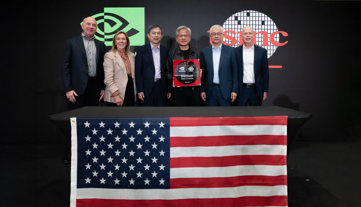
On October 17, 2025, Nvidia announced that it had produced its first Blackwell-series chip wafer, made by TSMC in the United States. This marks an important milestone for a major AI hardware company. It advances both its chip design and strengthens supply chain resilience in a crucial industry. For technology watchers and business leaders, this development shows how essential AI-ready processors and their manufacturing are becoming in global strategy.
What is the Blackwell wafer?
Blackwell refers to Nvidia’s next-generation AI architecture. It is designed to power large language models (LLMs), high-performance computing, and data-center inference workloads. The term “wafer” here means a full production slice of silicon that contains many chips, rather than just one packaged product. By working with TSMC in the US, Nvidia gains better control over production and possibly lowers shipping and trade risks. This partnership also allows for quicker development of its AI hardware. These wafers are important because AI tasks require more transistors, higher memory bandwidth, and energy-efficient processing, which wafer-level production can provide.
Why the US-TSMC partnership is strategic
MADE IN AMERICA: Nvidia and TSMC unveil first Blackwell chip wafer made in U.S. https://t.co/DxrJ989iZF
— Rapid Response 47 (@RapidResponse47) October 17, 2025
TSMC is the world’s leading contract chip maker. By partnering in the US, Nvidia secures a supply channel that is less vulnerable to geopolitical issues. Producing the wafer in the US also appeals to customers and governments that are concerned about reliance on offshore manufacturers. Furthermore, it highlights that progress in AI hardware is not just about chip design, but also about where and how those chips are made. The US push for advanced semiconductor manufacturing, backed by incentives like the CHIPS Act, aligns directly with Nvidia’s efforts. This combined approach of advanced architecture and domestic production may transform both technological innovation and the global economy.
In a broader sense, this partnership also represents a new phase of industrial cooperation. For decades, chip production has been centered in Asia, mainly in Taiwan and South Korea. By moving part of this process to the United States, companies like Nvidia and TSMC are helping create a more balanced and resilient global tech infrastructure. It also encourages the growth of skilled jobs, training, and research inside the US. These investments are not only technical but also political, as they aim to protect supply lines and prevent future chip shortages.
This move could inspire other technology companies to explore similar partnerships, spreading chip manufacturing capacity across several regions instead of depending on one. Such diversification helps stabilize global markets and ensures that innovation continues even during political tensions or natural disruptions. In short, Nvidia and TSMC’s collaboration is more than a manufacturing milestone — it is a sign that the world’s most powerful tech firms are learning to combine science, business, and strategy in a smarter and safer way.
TSMC is the world’s leading contract chip maker. By partnering in the US, Nvidia secures a supply channel that is less vulnerable to geopolitical issues. Producing the wafer in the US also appeals to customers and governments that are concerned about reliance on offshore manufacturers. Furthermore, it highlights that progress in AI hardware is not just about chip design, but also about where and how those chips are made. The US push for advanced semiconductor manufacturing, backed by incentives like the CHIPS Act, aligns directly with Nvidia’s efforts. This combined approach of advanced architecture and domestic production may transform both technological innovation and the global economy.
In a broader sense, this partnership also represents a new phase of industrial cooperation. For decades, chip production has been centered in Asia, mainly in Taiwan and South Korea. By moving part of this process to the United States, companies like Nvidia and TSMC are helping create a more balanced and resilient global tech infrastructure. It also encourages the growth of skilled jobs, training, and research inside the US. These investments are not only technical but also political, as they aim to protect supply lines and prevent future chip shortages.
MADE IN AMERICA: Nvidia and TSMC unveil first Blackwell chip wafer made in U.S. https://t.co/DxrJ989iZF
— Rapid Response 47 (@RapidResponse47) October 17, 2025
What this means for AI hardware and products
With the Blackwell architecture and improved wafer production, several benefits are expected: –
- More efficient AI training/inference: Blackwell aims to run LLMs more efficiently, using less power and providing faster results.
- Higher scale deployment: Wafer-level production can reduce the cost per chip, enabling the use of more data-center GPUs or accelerators.
- Shorter innovation cycle: Local manufacturing in the US means faster feedback and quicker updates, leading to better integration between design and production.
- Competitive edge: Nvidia might maintain or strengthen its leadership in AI infrastructure by managing both architecture and supply.
For industries such as cloud computing, scientific simulation, autonomous vehicles, and robotics, this advancement could lead to faster innovation and broader deployment of larger AI models.
Reuters
Technical highlights of the announcement
While full details remain confidential, some key technical points have emerged:
- The wafer uses TSMC’s advanced node, likely 3 nm or better, which allows for greater transistor density.
- Production took place in the US, which is uncommon among top AI chip manufacturers.
- The Blackwell architecture likely includes on-chip memory, improved connections, and better tensor computing units.
- Nvidia emphasized that this wafer is a foundational component for future products, not just a one-time effort. Though full benchmarks are not available yet, analysts expect Blackwell to provide 2-3 times the efficiency or performance compared to the previous Hopper or Ada Lovelace families, which already support many of today’s leading AI tasks.
Challenges ahead
Despite this significant progress, some challenges remain:
- Yield and reliability: New node wafers often face yield losses and manufacturing flaws; scaling up to large-scale production can be difficult.
- Cost and supply chain: Making advanced wafers in the US is costly, so pricing must be managed to stay competitive.
- Customer adoption: Data-center operators will look at not just performance but also the overall cost, the software ecosystem, and product availability.
- Global competition: Other companies, like AMD, Intel, and China’s SMIC, are developing their own architectures and designs; Nvidia needs to stay ahead.
Implications for global tech and industry
This announcement has broader effects beyond just Nvidia:
- Semiconductor geopolitics: US wafer manufacturing, along with advanced AI architecture, is changing the dynamics of the global chip supply.
- AI democratization: As chips become more efficient and cheaper, more organizations, including startups, universities, and governments, may gain access to high-quality AI hardware.
- Software-hardware co-design: With architecture and production closely linked, we may see more platforms optimized in a way that the hardware is tailored for specific AI models and tasks.
- Energy and sustainability: The power draw of AI data centers is a major concern. More efficient hardware can help lower energy use and support the environmental sustainability of AI growth.
How this impacts you (or typical users)
Even if you are not involved in a data center, you may experience indirect benefits:
- Faster apps: AI-based tools, such as those for editing, summarization, and design, may become more responsive.
- Edge devices: As chips become smaller and cheaper, more advanced AI could operate locally on devices, reducing the need for cloud reliance.
- Innovation cycle: Smaller firms may gain access to more powerful hardware sooner, speeding up new startups and product development.
Nvidia's CEO thoughts on this
Conclusion
The reveal of Nvidia’s Blackwell wafer, made by TSMC in the US, is not just a chip news story. It marks a shift in how AI hardware is built, where it is made, and how widely it may be used in the future. This is important for tech, business, and society. It means better AI, larger models, and possibly a fairer environment for innovation.
If you follow the development of AI, watch what happens after Blackwell: how it gets into products, which workloads benefit first, and how the ecosystem around it (software, data centers, supply chain) changes. We are in a hardware moment that could shape the next decade of AI.