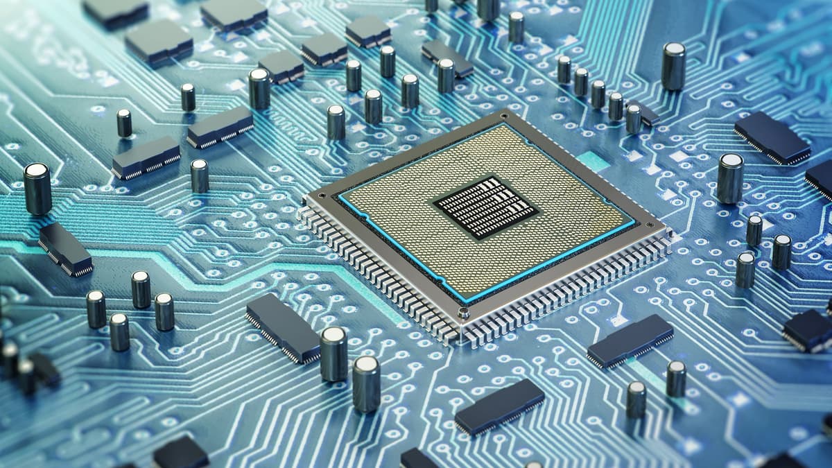
Scientists at Fudan University have created a working memory chip that combines atom-thin 2D materials with standard silicon circuitry. This is an important step toward real devices that use 2D semiconductors for faster, lower-power electronics. The team named their approach ATOM2CHIP and demonstrated a MoS₂-based memory array integrated on a standard CMOS die. This advance tackles long-standing challenges of incorporating 2D materials into mainstream chipmaking.
What are 2D materials, quick and clear
Two-dimensional (2D) materials are sheets that are only a few atoms thick. Graphene is the most well-known, but others like molybdenum disulfide (MoS₂) have useful electrical properties for semiconductors. Because they are so thin, 2D materials can be flexible and display unique electronic effects that bulk materials do not show. Engineers have been interested in using them for years, but getting them to work well on silicon chips has been a tough challenge.
The main achievement: ATOM2CHIP
Fudan’s team created a way to deposit a MoS₂ layer directly on a 0.13-micron CMOS silicon chip while protecting it during processing. They addressed issues like surface roughness and heat damage by using protective packaging and a conformal adhesion process. The result is a hybrid device: a 2D NOR flash memory array that operates alongside conventional CMOS control logic on the same chip. This is the first time a fully functional 2D memory array has been integrated directly with silicon logic at this level.
What the tests showed
In lab tests, the hybrid chip displayed strong performance: high manufacturing yield, very fast read/write speeds, long endurance, and ultra-low energy consumption per bit. Reported numbers include read/write speeds nearing 20 nanoseconds, endurance exceeding 100,000 cycles, and energy use measured below a picojoule per bit. The chip also supports 32-bit random access, meaning it can function like standard memory in many computing systems. These results make the device competitive with current flash memory in some areas.
Why this could change the industry
Integrating 2D materials with silicon could allow engineers to add new features without redesigning entire production lines. It opens up possibilities for lower power and faster memory for edge devices, sensors, wearables, and AI accelerators. Instead of further shrinking transistors, designers could add atom-thin layers to existing chips for new improvements. If manufacturers can implement similar modules, we may see a new category of hybrid chips that combine silicon’s reliability with the unique characteristics of 2D materials
Main challenges remaining
A promising lab demonstration is not the same as mass production. Several obstacles still exist:
- Scaling to wafers: The method must work uniformly across large wafers, not just small test chips.
- Material supply and quality: The industry needs reliable, high-quality 2D material production at scale.
- Long-term stability: Atom-thin layers can be sensitive to moisture, heat, and defects; packaging must shield them.
- Tooling and process changes: Foundries require equipment and procedures that handle atom-thin films without contamination or damage. Cost and yield: The economics must be better than alternatives for the industry to make the switch.
How industry might adopt it first
Real-world use may start in niche areas where low power and small size are most important: wearable electronics, sensors, medical devices, and specialized AI chips. As confidence increases, major companies could incorporate 2D modules into standard production as optional layers, similar to how new memory or RF modules are added today. Partnerships between universities, equipment suppliers, and foundries will be crucial to transition from lab work to manufacturing.
Quick technical comparison (table)
| Feature | Conventional Flash | Fudan 2D-CMOS Hybrid |
|---|---|---|
| Read/write speed | µs to ms | ~20 ns |
| Energy per bit | pico–nanojoules | < 1 pJ |
| Endurance | 10k–100k cycles | >100k cycles |
| Integration | Mature fabs | New module integration needed |
Watch here
Conclusion
Fudan’s ATOM2CHIP demonstrates that 2D materials can be used with traditional silicon to create actual devices. The prototype shows that atom-thin memory can be fast, durable, and energy-efficient on a CMOS platform. There are still major engineering and cost challenges ahead, but the way forward for hybrid 2D-silicon chips is clearer now. If the industry can scale this method, the next generation of devices might be lighter, faster, and significantly more power-efficient.